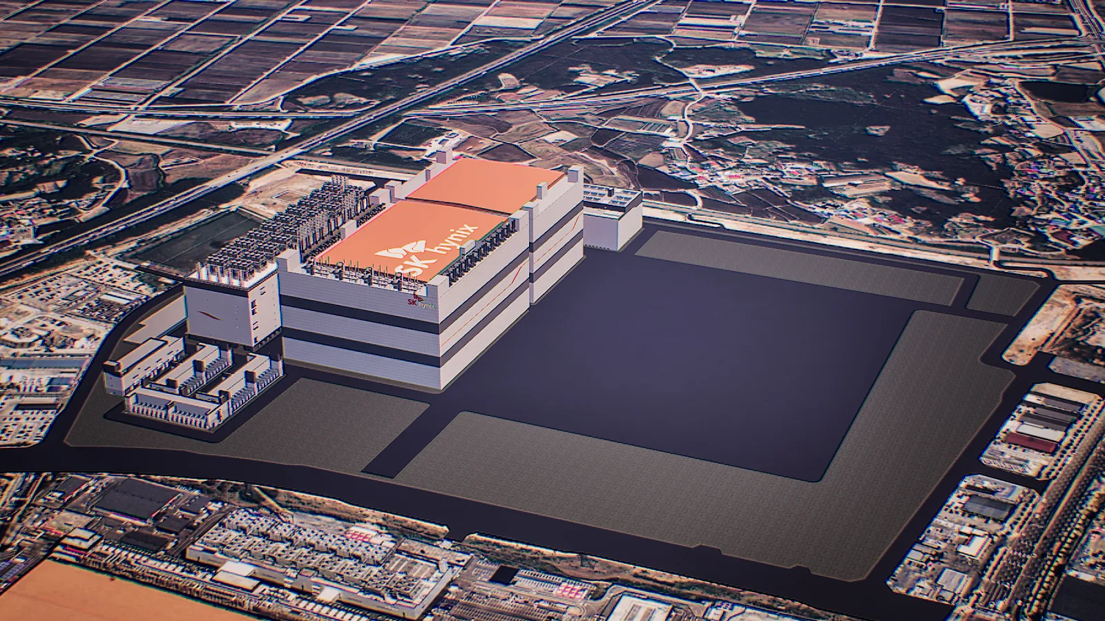
In a move that signals a tectonic shift in the global semiconductor landscape, South Korean memory giant SK Hynix has announced a staggering mid-to-long-term investment plan totaling 1,100 trillion KRW (approximately $713 billion). This monumental capital injection is designed to solidify the company’s dominance in the AI-driven memory market by aggressively expanding its manufacturing footprint across South Korea. To fuel this unprecedented growth, the company has confirmed its intent to list on the Nasdaq exchange in the United States, seeking to raise roughly 45.45 trillion KRW ($29 billion) in capital.
As SK Hynix pivots toward the mass production of next-generation high-bandwidth memory (HBM), the global financial community is watching closely. While the investment underscores an unwavering confidence in the longevity of the AI infrastructure boom, it also highlights the precarious nature of the current semiconductor cycle, with analysts debating the potential fallout should global AI spending experience a correction.
The Strategic Blueprint: A Multi-Phase Industrial Transformation
SK Hynix’s expansion is not merely a capacity increase; it is a fundamental re-engineering of the company’s domestic manufacturing presence. The strategy focuses on three primary geographic clusters in South Korea, each designed to address specific segments of the memory market.

1. The Yongin Semiconductor Cluster
The crown jewel of the investment is the Yongin semiconductor cluster, which will receive an allocation of 600 trillion KRW (~$390 billion). Recognizing the urgency of the AI supply crunch, SK Hynix has accelerated its construction timeline, now aiming to complete its fourth fabrication facility (fab) by 2033—a full 12 years ahead of the original projection. This facility will be instrumental in meeting the explosive demand for advanced DRAM and AI-centric memory solutions.
2. The Cheongju NAND and Packaging Hub
The company is dedicating 100 trillion KRW (~$65 billion) to the Cheongju region. This capital will be split between the M17 NAND production fab and a massive 20 trillion KRW investment in the P&T7 advanced packaging facility. This investment is critical; as AI chips grow in complexity, the ability to package them effectively—ensuring thermal management and efficient data transfer—has become as important as the silicon itself.
3. The Southwestern Expansion
Rounding out the domestic strategy, SK Hynix will deploy 400 trillion KRW (~$260 billion) across the Southwestern region of South Korea. This phased approach allows the company to remain agile, scaling its capacity in response to real-time fluctuations in market demand and cash flow.

To support these industrial efforts, the parent organization, SK Group, has committed to developing 15 gigawatts of AI-dedicated data center infrastructure throughout the country, ensuring that the physical hardware and the energy requirements for AI compute are integrated seamlessly.
Chronology of the Expansion
- Mid-2024: SK Hynix begins internal planning for a massive, multi-decade capital expenditure (CAPEX) cycle.
- Early 2025: Initial planning for the acceleration of the Yongin cluster is finalized as AI demand projections for 2026–2030 are revised upward.
- Q2 2026: SK Hynix successfully ships 12-layer HBM4E samples to key hyperscaler partners, signaling the move toward next-generation memory standards.
- July 10, 2026: Target date for the listing of American Depositary Receipts (ADRs) on the Nasdaq Global Select Exchange, marking a historic shift in the company’s financial structure.
- 2027–2033: Implementation of the phased investment plan, with sequential openings of new fabs in Yongin, Cheongju, and the Southwestern clusters.
Technical Prowess: The HBM4E Advantage
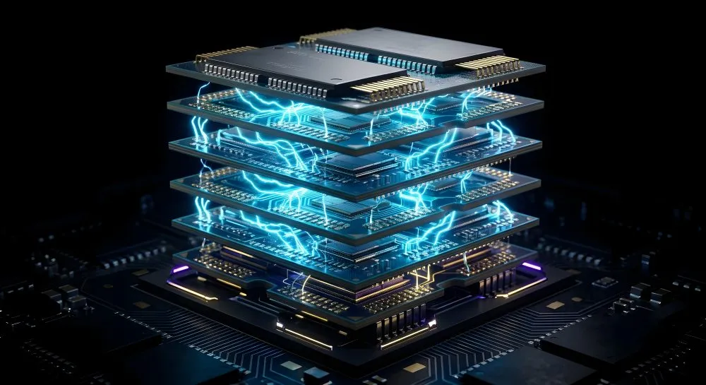
The technical impetus for this spending spree is the evolution of High-Bandwidth Memory (HBM). Unlike conventional DRAM, HBM is manufactured by stacking chips using through-silicon vias (TSVs). This design increases chip size and complexity, resulting in a lower number of usable chips per wafer. Consequently, to maintain the same volume of usable memory, manufacturers must invest significantly more in wafer manufacturing capacity.
SK Hynix is currently leading this transition with its 12-layer HBM4E memory. These modules boast data processing speeds of 16 gigabits per second per pin, offering a 20% improvement in power efficiency compared to their predecessors. Central to this success is the company’s proprietary Advanced Mass Reflow Molded Underfill (MR-MUF) technology. By increasing heat resistance by 17%, this process allows for the reliable operation of memory stacks in high-performance computing (HPC) environments where thermal throttling is a constant risk.

Official Rationale: The "AI Deployment" Era
During a national briefing on advanced industrial strategy, SK Hynix President and CEO Kwak Noh-Jung provided a clear justification for the scale of this investment.
"The AI industry has moved beyond the training phase and entered an era in which AI services are being deployed at scale," Kwak stated. He argued that current supply constraints are not merely a temporary bottleneck but a structural shift in the market. "The Yongin site alone will not satisfy future market needs," he added. "We will re-establish Cheongju as a key hub for driving the competitiveness of the memory semiconductor industry in Korea, ensuring we have the packaging and NAND capabilities to support the entire AI ecosystem."
Ahn Hyun, President and Chief Development Officer, underscored the collaborative nature of this effort, noting that the company is working closely with its primary customers to ensure that these new HBM4E products move quickly from the sampling phase to full-scale mass production.

Financial Implications: The Nasdaq Listing
The decision to list on the Nasdaq is a bold strategic maneuver designed to diversify the company’s capital base. By targeting a $29 billion raise, SK Hynix is significantly outpacing initial market estimates. This capital will be utilized not only for the construction of buildings but for the acquisition of the ultra-sophisticated lithography and testing machinery required for modern semiconductor fabrication.
The listing will likely alter the competitive dynamics of the global memory sector. By flooding the market with increased supply, SK Hynix may exert downward pressure on component prices, a move that could compress the margins of competitors like Micron and Samsung. For investors, the ADRs provide a new avenue to participate in the memory cycle, potentially shifting capital flows away from other players in the industry.
Risk Assessment: The Shadow of a Spending Contraction
Despite the optimism, a sense of caution permeates the industry. The growth of the semiconductor sector is currently tied to the capital expenditure of hyperscalers—the massive cloud providers building the world’s AI infrastructure.

Nomura Securities projects that global investment in AI data centers will soar from $466 billion in 2025 to a staggering $3.379 trillion by 2030. While this 48% compound annual growth rate is lucrative, the Bank for International Settlements (BIS) has sounded an alarm in its 2026 annual report. The BIS warns that if the current wave of AI implementation fails to generate sufficient financial returns to cover the massive upfront infrastructure costs, a sudden contraction in spending is inevitable.
Such a scenario would have ripple effects far beyond the semiconductor industry. Construction, energy, and supply chain logistics—all of which are currently benefiting from the data center building boom—would face immediate disruption. Furthermore, the reliance on debt to fund these capital-intensive projects creates a systemic risk; a market downturn could lead to widespread corporate defaults, exacerbating inflationary pressures and complicating the role of central banks in managing the global economy.
Conclusion
SK Hynix’s $713 billion investment is a defining moment for the company and the broader tech industry. By doubling down on its home turf while simultaneously tapping into U.S. capital markets, the company is preparing for a future where AI-driven memory is the backbone of the global economy. Whether this bet results in a new era of prosperity or a cautionary tale of excessive capacity remains to be seen. For now, however, SK Hynix is positioning itself to be the indispensable provider of the building blocks for the next decade of human technological advancement.