By Cadence Design Systems | August 26, 2026
The transition from theoretical AI models to robust, real-world physical systems has become the defining engineering challenge of the mid-2020s. While generative AI models dominate headlines with their prowess in text and image synthesis, the next frontier—Physical AI—requires silicon that can perceive, reason, and act in real-time within the unforgiving constraints of the physical world.
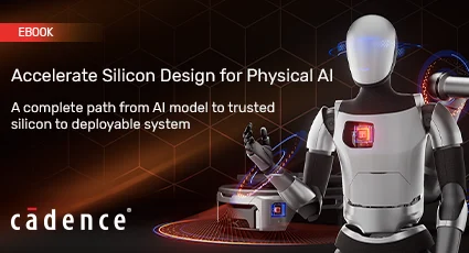
As engineering teams strive to move beyond the "one-processor" paradigm, they are encountering a complex convergence of architectural, security, and supply chain hurdles. To address these, Cadence Design Systems has unveiled a comprehensive framework designed to navigate the path from AI model inception to trusted, deployable silicon.
The Core Challenge: Why Traditional Architectures Fail
For decades, the semiconductor industry relied on the monolithic processor model. Whether CPU, GPU, or early-stage NPU, these chips were designed for high-throughput, general-purpose tasks. Physical AI—the intelligence embedded in robotics, autonomous vehicles, and industrial automation—shatters this model.
Physical AI systems operate under extreme conditions. They must process multi-modal sensor data, execute inference with sub-millisecond latency, and maintain energy efficiency that permits operation on edge-device power budgets. When a robotic arm misses a nuance in its environment, the cost is not a dropped frame or a hallucinated sentence; it is a physical failure.
This workload diversity has created a "dead zone" between the high-level code developed by data scientists and the physical silicon required to run it. Bridging this gap requires more than just faster transistors; it necessitates a fundamental rethinking of how hardware interacts with the software lifecycle.
Chronology: The Evolution Toward Heterogeneous Computing
To understand the current state of the industry, one must look at the timeline of hardware adaptation over the last five years:
- 2021–2022: The Era of Software-Defined AI. Organizations focused heavily on software frameworks, assuming that general-purpose GPUs would scale to meet every AI demand.
- 2023–2024: The Wall of Latency. As models grew more complex, teams realized that "off-the-shelf" hardware could not meet the real-time requirements of physical robots and safety-critical edge systems.
- 2025: The Rise of Custom Silicon. Companies began aggressively pursuing application-specific integrated circuits (ASICs) and custom silicon to optimize for specific neural network architectures.
- 2026: The Infrastructure Shift. The current landscape is defined by the need for "Trusted Silicon." With the rise of multi-vendor supply chains, security is no longer an add-on—it is a foundational requirement that must be baked into the silicon from the pre-RTL (Register Transfer Level) design phase.
Supporting Data: The Architecture Trade-off
The industry is currently locked in a debate between the Monolithic approach and the Chiplet/Multi-die approach. Cadence’s new framework provides data-driven guidance on how to evaluate these paths:
The Monolithic Advantage
- Latency: Minimal interconnect overhead, ideal for ultra-low latency applications where every nanosecond counts.
- Simplicity: Easier physical verification and a more straightforward manufacturing flow for smaller, highly optimized designs.
- The Downside: Yield sensitivity. As chip sizes increase, the probability of a defect renders the entire die useless, significantly increasing costs for complex, large-scale AI chips.
The Chiplet/Multi-die Advantage
- Scalability: Allows architects to mix and match process nodes (e.g., a 3nm compute die with a 7nm I/O die), optimizing for both performance and cost.
- Reusability: Once a high-performing "AI core" chiplet is designed, it can be reused across different system architectures, drastically reducing time-to-market.
- The Downside: Complexity in integration. Advanced packaging (2.5D/3D) and inter-die communication protocols introduce new variables in thermal management and signal integrity.
Official Perspective: Engineering for the Full Lifecycle
"The goal is a clear, lower-risk path from concept to production silicon," notes the technical leadership at Cadence. "Teams shouldn’t be wasting their finite engineering hours rebuilding foundational infrastructure. Instead, they should be focusing on differentiation—the unique IP that makes their specific AI agent perform better than the competition."
The framework provided by Cadence emphasizes that "Trusted Silicon" is not a static state. It is a lifecycle requirement.
- Boot-time Security: Ensuring the chip only executes signed, verified firmware.
- Operational Integrity: Monitoring for side-channel attacks and hardware-level tampering during the system’s active life.
- End-of-Life: Ensuring that as devices are decommissioned, sensitive IP and user data are cryptographically erased from the silicon.
Implications: The Future of Deployment
The shift toward this structured, framework-based approach to silicon design will have three primary implications for the technology sector:
1. The Democratization of Custom Silicon
By providing a blueprint for heterogeneous inference, smaller firms can now consider custom silicon paths that were previously the domain of hyperscalers. This will likely lead to an explosion in specialized AI hardware tailored to niche industrial and scientific applications.
2. Supply Chain Resilience
In a world of multi-vendor supply chains, the ability to anchor trust in hardware—regardless of where the individual components were manufactured—is a geopolitical and commercial imperative. The emphasis on hardware-level security ensures that even if a supply chain is fragmented, the final system remains a "known good" entity.
3. A Focus on Differentiation
When the foundational infrastructure—the "plumbing" of AI deployment—is standardized through proven frameworks, the competitive landscape shifts. Value will no longer be determined by who can build a chip, but by who can build the most efficient, safe, and intelligent system.
Conclusion: Moving from Concept to Production
The path from an AI model to a physical system is no longer a linear line; it is a complex, iterative loop that requires constant synchronization between hardware architects and software developers. The transition to heterogeneous, secure, and scalable silicon is inevitable for any organization serious about the future of Physical AI.
As the industry matures, those who adopt a "lifecycle-first" mindset—prioritizing integration risk reduction and infrastructure reusability—will be the ones to dominate the next decade of automation. By right-sizing inference to the specific application, rather than trying to force-fit models into legacy architectures, engineering teams can finally unlock the true potential of the machines they build.
For those interested in implementing this framework, Cadence provides a detailed guide on navigating these architectural choices, available for architects and system designers looking to streamline their path from concept to silicon production.