In the demanding environment of modern industrial automation, the 24V DC power supply serves as the lifeblood of control panels, communication modules, and sophisticated edge AI hardware. From industrial cameras to high-speed inference boxes, these systems rely on stable power to maintain uptime. However, the industrial floor is a hostile electrical environment. Engineers must contend with a convergence of threats—reverse polarity, hot-plugging transients, voltage surges, and sudden load fluctuations—that can turn a standard power rail into a point of failure.
Reliability is not achieved by selecting a single "best" component; it is an emergent property of the entire power path. A system is only as robust as its weakest link, and treating the power signal chain as a series of isolated components is a recipe for field failure.
The Anatomy of the Power Path
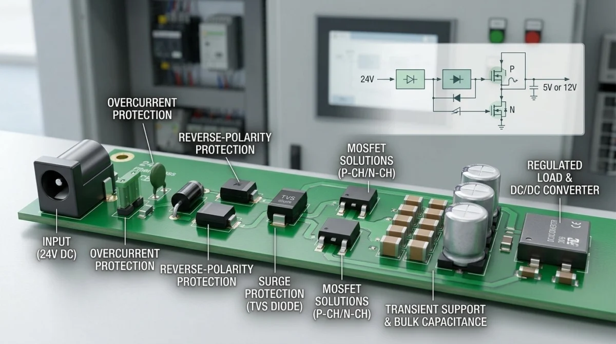
The power signal chain begins at the entry point, typically protected by a fuse or a Positive Temperature Coefficient (PTC) device. From there, the path flows through a Transient Voltage Suppression (TVS) diode and a reverse-polarity protection stage, followed by input capacitance, before finally reaching the DC/DC converter and the load.
Figure 1 illustrates this progression. Each stage must be meticulously coordinated. If the protection devices are not impedance-matched or if the thermal dissipation is miscalculated, the interaction between these components can lead to unexpected resonance or catastrophic failure.

Defining Electrical Threats: The Engineer’s Checklist
Before a single component is sourced, the design engineer must categorize the threats specific to the application. A systematic approach to failure modes—such as overcurrent, overvoltage, and inductive kickback—is essential for selecting the appropriate protective silicon.
| Fault | Protection Task | Key Component |
|---|---|---|
| Reverse Polarity | Blocking current from incorrect orientation | Series diode, Schottky, or MOSFET |
| Surge/Transient | Clamping sudden voltage spikes | TVS Diode with upstream impedance |
| Reverse Current | Stopping backward current flow | Back-to-back MOSFETs/Ideal-diodes |
| Inrush Current | Limiting power-on current spikes | Bulk capacitance & MOSFET SOA |
| Inductive Kickback | Absorbing energy from motors/coils | Freewheeling or clamping diodes |
Reverse-Polarity Protection: Diode vs. MOSFET
The choice between a simple diode and an active MOSFET is a classic engineering trade-off between simplicity and efficiency.
The Diode Solution
Standard rectifier and Schottky diodes are the "plug-and-play" solutions for reverse-polarity protection. Schottky diodes are favored for their low forward voltage drop ($V_F$), which significantly reduces conduction losses. However, they are prone to higher leakage currents, which escalate exponentially as temperatures rise. Engineers must calculate the total thermal load—incorporating duty cycles and thermal resistance—rather than relying solely on leakage specifications.
The MOSFET Advantage
For higher-efficiency designs, P-channel or N-channel MOSFETs are superior. A P-channel MOSFET simplifies gate control but requires careful attention to $VGS$ limits at the 24V input range. N-channel MOSFETs offer the lowest $RDS(on)$ but necessitate the complexity of a charge pump or dedicated gate driver.

When current must be blocked in both directions, engineers employ back-to-back MOSFET configurations. This setup effectively isolates the load from the input, providing a robust, low-loss barrier that a standard diode cannot match.
TVS Selection: Matching the Voltage Window
A common pitfall in power path design is misinterpreting the ratings of a TVS diode. Engineers often confuse the Breakdown Voltage ($V_BR$) with the Clamping Voltage ($VC$). While $VBR$ indicates when the diode begins to conduct, $V_C$ is the actual voltage the downstream components will experience during a surge.
To ensure safety, the maximum steady-state input voltage must remain below the Maximum Working Voltage ($V_RWM$), and the worst-case $V_C$ must stay safely below the absolute maximum input rating of the DC/DC converter. Furthermore, TVS diodes are not a substitute for fuses; they are designed for transient suppression. In the event of a sustained overvoltage, a TVS will eventually reach its thermal limit and fail.
The Role of Capacitance: Balancing Support and Inrush
The input capacitor bank serves two masters: it filters high-frequency noise and provides bulk energy storage. Multi-layer ceramic capacitors (MLCCs) are excellent for high-frequency bypass, but their effective capacitance drops drastically under DC bias. Conversely, aluminum electrolytic capacitors offer the energy density required for load steps but are limited by ESR and temperature-related degradation.

A sophisticated design uses a hybrid approach, combining MLCCs for noise and electrolytic capacitors for bulk energy. However, this creates a secondary challenge: inrush current. Large capacitor banks can trigger protection circuits or stress MOSFETs during power-on, requiring careful management of the charging rate.
Case Study: A 24V Industrial Input Design
Consider a system designed to handle a 1kV surge (based on IEC 61000-4-5) with a 42Ω source impedance. The design follows a rigorous six-step methodology:
- Goal Setting: Define the operating voltage window (e.g., 24V ±10%).
- Loss Analysis: Compare the conduction losses of a Schottky diode vs. a MOSFET.
- Component Rating: Verify $RDS(on)$, $VDS$ margins, and Safe Operating Area (SOA).
- TVS Calibration: Calculate the worst-case $V_C$ to protect the downstream DC/DC converter.
- Capacitance Sizing: Balance effective MLCC capacitance against inrush current constraints.
- Validation: Conduct thermal testing and stress tests for load steps and reverse polarity.
In our worked example, calculations show that a MOSFET provides a significant efficiency gain over a Schottky diode (0.27W vs 1.5W of loss). However, the margin between the TVS clamping voltage (38V) and the converter’s max rating (40V) is perilously thin. This highlights the need for secondary verification—a step often overlooked by less experienced design teams.
Implications for Industry
The trend toward miniaturization in industrial edge AI and robotics has made the power path more vulnerable than ever. As components shrink, their tolerance for thermal stress and voltage transients decreases. Companies like Unikeyic are addressing this by providing engineers with parametric tools to filter components based on specific design requirements, such as $RDS(on)$ at high temperatures or $VGS$ limits.

The implications for developers are clear: "Design for reliability" is not a marketing slogan—it is a technical requirement. Integrating MOSFETs, diodes, TVS devices, and capacitors into a single, coordinated signal chain is the only way to ensure that a piece of equipment will survive the unpredictable realities of an industrial environment.
Conclusion: The Integrated Approach
Reliable power path design is not about selecting the most expensive parts; it is about understanding how components interact under stress. By considering the entire chain—from the input fuse to the final load—engineers can prevent the "death by a thousand cuts" that leads to field failure. As the industrial sector continues to embrace AI and smart manufacturing, the ability to design robust, efficient, and protected power paths will remain a cornerstone of engineering excellence.
For those seeking to optimize their supply chain, utilizing comprehensive distribution platforms allows for the sourcing of high-performance components that meet these strict design criteria. Whether it is high-precision ceramic capacitors or low-loss MOSFETs, the foundation of a reliable system begins with the quality of the components selected and the rigorous methodology applied to their integration.