The rapid evolution of artificial intelligence models has triggered a seismic shift in semiconductor engineering. As Large Language Models (LLMs) and generative AI architectures balloon in size, the traditional bottleneck—the "memory wall"—has moved from a nuisance to a critical existential threat for hardware designers. According to Pascal Vivet, program manager for advanced programs at the French research institute CEA-Leti, the industry is entering an era where hardware design can no longer treat packaging as an afterthought. Instead, 3D integration and chiplet-based architectures have become the fundamental bedrock of modern AI system design.
Main Facts: The New Frontier of Silicon Density
The core challenge facing engineers today is a three-pronged conflict: the need to place massive amounts of memory (often in the hundreds of gigabytes or even terabytes) closer to the processor, the necessity of moving data with minimal energy consumption, and the rising peril of extreme power density.
"3D technology is key," Vivet told EE Times. "It allows the industry to scale horizontally, vertically, and to assemble the best technology for chiplet partitioning in an open ecosystem."

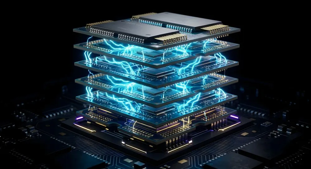
The industry is currently moving away from the conventional High-Bandwidth Memory (HBM) model, which, despite its name, is hitting a physical wall. While HBM successfully stacks DRAM beside processors, the connection remains a side-by-side lateral interface. This distance limits the energy efficiency and the total bandwidth available. Leti’s vision, and that of the broader vanguard of semiconductor research, is to move toward "slower, wider, and closer" interfaces—stacking memory directly atop compute engines or integrating them via ultra-dense, low-energy vertical interconnects.
Chronology: The Evolution of Advanced Packaging
The transition from monolithic dies to advanced packaging has been a gradual, multi-decade process that has accelerated sharply since 2020:
- Pre-2015: Monolithic system-on-chip (SoC) design dominated. Scaling was achieved primarily through process node shrinks.
- 2016–2020: The rise of 2.5D packaging and HBM. Interposers became the standard for connecting memory and compute, allowing for higher data throughput.
- 2021–2023: Introduction of 3D-IC and initial hybrid bonding. The focus shifted toward reducing the physical distance between dies to lower power consumption during data transfer.
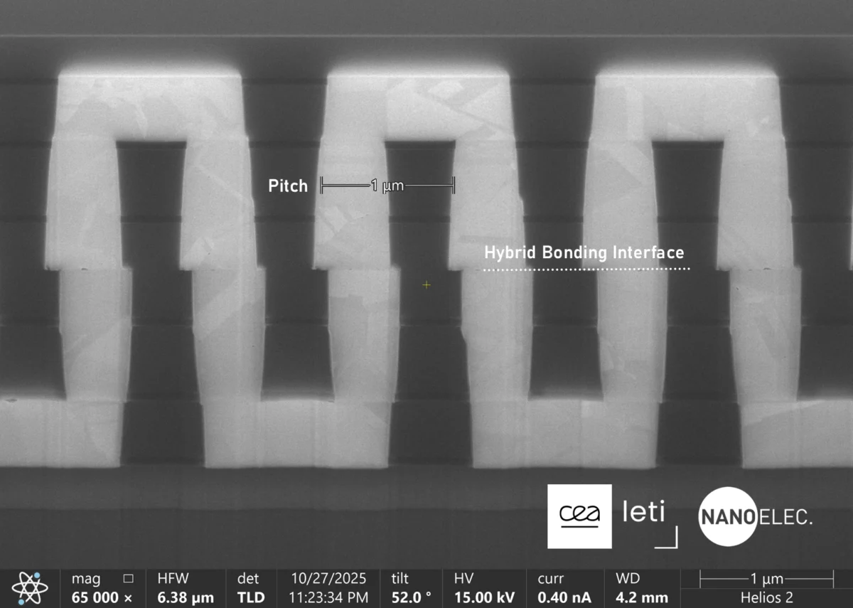
- 2024–2026 (Present): The emergence of "System-on-Interposer" and advanced hybrid bonding, with research demonstrations achieving 1-micron pitch interconnects.
- 2027 and Beyond: Anticipated industry-wide adoption of wafer-to-wafer hybrid bonding (targeting 200 nm pitch) and integrated power management directly within the 3D stack.
Supporting Data: The 3D Integration Toolbox
CEA-Leti is currently developing a comprehensive "toolbox" designed to facilitate these architectures. At the heart of this research are interconnects that defy traditional manufacturing constraints. Recent demonstrations have showcased die-to-wafer (D2W) hybrid-bonding interconnects at a 1-micron pitch, with research roadmaps aiming for a wafer-to-wafer (W2W) target of 200 nm.

This density is essential for managing the energy-per-bit cost of AI inference. By moving from long, resistive horizontal traces to short, vertical pillars, the energy required to move a single byte of data can be reduced by orders of magnitude. Furthermore, the use of virtual prototyping—where software models are annotated with specific thermal and electrical data—has become the new standard for pre-silicon validation. These tools allow designers to simulate the thermal dissipation profile of a 3D-stacked chip long before a single mask is drawn.
Official Responses and Strategic Perspectives
For Pascal Vivet, the most daunting hurdle is not the physical stacking of silicon, but the "early partitioning" of the system. "The most difficult part is early partitioning of the system in terms of technology layers and functions," Vivet noted.
Traditionally, chip design follows a linear path: architecture, then circuit design, then packaging. In the world of AI accelerators, this sequence is obsolete. Designers must now conduct "co-optimization," where thermal, electrical, and cost considerations are evaluated concurrently.

Regarding the thermal envelope, Vivet highlighted that power density, rather than the raw power budget, is the true limiting factor. "Water cooling defines the maximum power density of the chip," he explained. This realization forces a design constraint: if a system cannot dissipate the heat generated by the 3D stack, the performance gains of that stack are neutralized. Consequently, engineers are exploring point-of-load power delivery, integrated passives, and even photonics to manage heat and signal integrity more effectively.
Implications: A New Era for Chiplet Ecosystems
The implications of this shift are profound, particularly for regional tech sovereignty and the democratization of AI hardware.
The Death of the Passive Package
The package is no longer a passive container for the chip; it is an active, functional component of the architecture. Advanced packaging now dictates the system’s performance ceiling. This necessitates a move toward "design-for-packaging" methodologies where the package and the silicon are co-designed from day one.

The Chiplet Paradigm
The push for 3D integration is intrinsically linked to the rise of open chiplet ecosystems, such as those governed by the UCIe (Universal Chiplet Interconnect Express) standard. For companies in Europe and beyond, this provides a vital strategic advantage: it allows smaller players to combine specialized IP blocks—such as custom AI accelerators—with commodity memory or I/O dies, without needing to manufacture every single component at the most expensive, leading-edge process nodes.
Thermal and Power Management
As we move toward "point-of-load" power delivery, the architecture of the power delivery network (PDN) must be redesigned. Future systems will likely feature power management functions integrated directly into the backside of the silicon, effectively turning the back of the die into a micro-power station. This reduces the impedance between the power source and the compute logic, further optimizing energy efficiency.
Sector-Specific Applications
While high-end data centers will push the boundaries of liquid-cooled, 3D-stacked memory-on-compute, other sectors face different mandates. Automotive, aerospace, and defense applications require high reliability and ruggedized designs. For these industries, 3D integration offers a path to integrate advanced features—such as edge AI inference capabilities—without requiring the extreme, exotic cooling solutions found in hyperscale data centers.

Conclusion: The Path Forward
The future of AI hardware will not be written by a single, faster processor or a denser memory module in isolation. It will be determined by the intelligence of the system-level integration. As CEA-Leti’s work underscores, the industry is transitioning from a "process-centric" world to an "architecture-centric" world.
The success of the next generation of AI will rely on the seamless marriage of thermal engineering, power distribution, and 3D interconnect density. By treating the package as the primary architectural constraint rather than a secondary assembly step, the semiconductor industry is laying the foundation for a future where AI models can grow in complexity without being stifled by the physical limitations of the chips that run them. The "memory wall" is being dismantled, one vertical interconnect at a time.