In a landscape dominated by the relentless pursuit of Moore’s Law, the semiconductor industry has reached a point of diminishing returns. For decades, the mantra was simple: shrink the transistor, increase the density, and performance will follow. However, as the industry hits the physical walls of atomic-level lithography, Huawei Technologies has emerged with a radical departure from conventional wisdom.
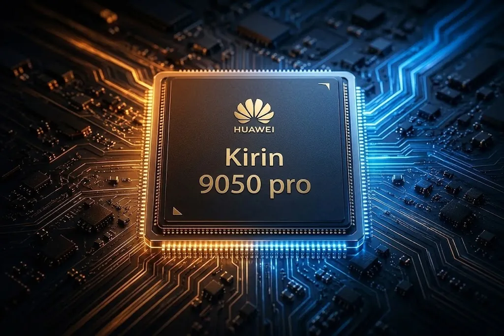
In early September 2026, alongside the debut of its groundbreaking tri-fold smartphone, the Mate XT 2, Huawei unveiled the Kirin 9050 Pro. This processor is not merely a generational upgrade; it is the first commercial realization of "Tau (τ) Scaling"—a design philosophy that prioritizes signal travel time over raw transistor size. By shifting focus from spatial geometry to temporal efficiency, Huawei is attempting to bypass the restrictive barriers imposed by Western sanctions on extreme ultraviolet (EUV) lithography.
The Main Facts: A Paradigm Shift in Processor Architecture
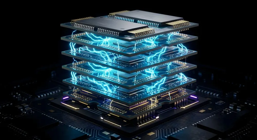
The Huawei Mate XT 2 is arguably the most ambitious foldable device ever brought to market, but its true significance lies under the hood. The Kirin 9050 Pro processor introduces "LogicFolding," a proprietary technique that stacks active silicon layers vertically.
Traditional chip design relies on horizontal routing—long, metallic "wires" that connect transistors across a flat plane. As chips have shrunk, these wires have become a bottleneck, increasing resistance and parasitic capacitance. Huawei’s LogicFolding replaces these horizontal paths with vertical connections, drastically reducing the physical distance signals must travel.

According to technical documentation presented at the 2026 IEEE International Symposium on Circuits and Systems by He Tingbo, president of Huawei’s semiconductor division, this approach reduces core routing lengths by 20% and slashes key timing paths by up to 70%. The result is a chip that operates with significantly lower energy consumption—66% lower for the NPU and 58% lower for the GPU—without relying on the high-voltage, high-clock-speed thermal profiles that typically plague high-performance silicon.
Chronology: The Road to LogicFolding
The genesis of this architectural pivot can be traced back to the intensifying U.S. export controls that effectively severed Huawei’s access to ASML’s cutting-edge EUV lithography equipment.
- 2023–2024: Huawei pivots toward deep research into domestic supply chain independence, realizing that 7-nm production via standard DUV (deep ultraviolet) lithography would eventually hit a performance ceiling.
- May 2026: He Tingbo introduces the "Tau Scaling Law" at the IEEE International Symposium, arguing that the future of compute is not just about the number of transistors, but the "temporal cost" of moving data between them.
- September 12, 2026: The Huawei Mate XT 2 officially launches in China, featuring the Kirin 9050 Pro. This serves as the "proof of concept" for vertical stacking and LogicFolding in a consumer-facing product.
- Late 2026: Huawei begins shifting its R&D focus toward achieving a 720-nm hybrid-bonding pitch by 2027, with long-term goals of mimicking 1.4-nm density by 2031 through continued vertical integration.
Supporting Data: Efficiency and Thermal Management
The performance metrics of the Kirin 9050 Pro are staggering, particularly when considering that they were achieved without access to the latest sub-5-nm EUV process nodes.
Huawei’s data indicates that the chip utilizes a nine-core CPU architecture with a primary core clocking at 3.1 GHz. The integrated Maleoon 920 GPU is capable of 50 million rays per second for hardware ray tracing, while the Da Vinci NPU enables the on-device execution of a 30-billion-parameter Mixture-of-Experts (MoE) AI model.

Perhaps most impressive is the energy efficiency. By focusing on "temporal scaling," Huawei has managed to keep thermal dissipation manageable. Instead of ramping up clock speeds—which generates exponential heat—the company has optimized the chip’s internal data paths to move information faster at lower voltages. This allows the Mate XT 2 to sustain high-performance tasks, such as real-time generative AI, for longer durations than its competitors, despite the inherent power challenges of driving a massive tri-fold display.
Official Responses and Industry Perspectives
The reception from the broader semiconductor community has been one of cautious observation. Mateo Valero, director of the Barcelona Supercomputing Center (BSC), highlights that while Huawei’s innovation is impressive, it represents a shift toward "full-stack orchestration."
"The transistor is important, but what matters now is how an entire system behaves," Valero told EE Times. "You have to co-design from the application all the way down to the transistor, software, system-on-chip architecture, and memory layout, or you run into bottlenecks elsewhere."
Huawei’s approach is inherently defensive. The company’s R&D expenditure reached 121.38 billion yuan (~$18.13 billion) in the first half of 2026—a 25.2% increase—as it pours capital into self-reliance. This spending has compressed net profit, which fell by 36% during the same period, signaling that Huawei is willing to trade short-term financial health for long-term technological sovereignty.

Implications: A New Era of Geopolitical Tech
The implications of LogicFolding extend far beyond a smartphone display. Huawei is signaling its intent to enter the enterprise AI compute market, directly challenging Nvidia. By 2030, the company plans to scale this architecture to its Ascend 990 AI chips.
1. The Death of Standard Instruction Sets?
Perhaps the most disruptive element is the rumored implementation of "LinxISA." By moving away from Arm—which is subject to U.S. regulatory oversight—and potentially RISC-V, Huawei is creating a proprietary ecosystem. LinxISA’s block-structured architecture, which processes instructions in batches rather than sequentially, is designed specifically to feed the high-bandwidth requirements of vertical-stacked chips.
2. Software Autonomy
The rollout of HarmonyOS 7, which is entirely free of open-source Android code, completes the "walled garden." By controlling the OS kernel, the file system (EROFS), and the underlying instruction set architecture, Huawei is building a vertical silo that is theoretically immune to external software sanctions.
3. The Foundries of the Future
Huawei’s work with SMIC and local etching/deposition suppliers like AMEC and NAURA is creating a "China-only" manufacturing ecosystem. While current yields for these complex 3D-stacked chips remain a point of concern—due to the extreme precision required in wafer thinning and copper pad alignment—Huawei is betting that the cost of domestic R&D will eventually be offset by the security of a closed supply chain.

Conclusion: The Road Ahead
The Huawei Mate XT 2 and the Kirin 9050 Pro represent a defiant response to the limitations imposed by the global trade war. By evolving from "shrinking transistors" to "compressing time," Huawei has identified a path that does not require the latest EUV lithography to achieve competitive performance.
However, the road remains fraught with obstacles. As Mateo Valero noted, "unless memory arrangement, compilers, and hardware scheduling are seamlessly orchestrated, isolated architectural tricks cannot overcome physical manufacturing constraints."
Whether Huawei can maintain this pace of innovation while absorbing the massive costs of full-stack development remains the industry’s most compelling question. For now, the Kirin 9050 Pro stands as a testament to what is possible when a company is forced to reinvent the fundamental physics of its product. As the industry watches, the "Tau Law" may well become the new North Star for those operating outside the traditional global semiconductor alliance.