By Teng Tang Yang, Senior Division Director of Product Marketing Division, UMC
Displays serve as the fundamental bridge between humanity and the digital realm. From the early, monochromatic cathode-ray tubes to the high-definition, flexible panels that define our current era, the evolution of display technology has been a relentless pursuit of clarity, power efficiency, and immersion. As we approach 2026, the industry is witnessing a shift that transcends simple screen size: we are moving toward a future where high-resolution, vibrant, and ultra-responsive interfaces are integrated into the smallest form factors imaginable, including AR/VR headsets and next-generation smart wearables.
At the heart of this revolution lies the Display Driver IC (DDIC). Often overlooked by the end consumer, the DDIC is the unsung hero of the modern digital experience. It acts as the crucial controller and interface between the graphics processor and the display panel, translating complex digital image data into precise pixel-driving signals. The quality of this translation directly dictates visual fidelity, device battery life, and the responsiveness of touch-enabled interfaces. As display technology migrates from conventional LCDs to sophisticated OLED and emerging micro-OLED architectures, the manufacturing requirements for these controllers are reaching new levels of complexity.

Main Facts: The Shift Toward AMOLED and Silicon-Based Integration
The most significant development in the current display landscape is the transition from passive-matrix architectures to active-matrix organic light-emitting diode (AMOLED) technology. Unlike passive-matrix (PMOLED) displays, which are limited in resolution and generally confined to small-screen applications, AMOLED displays utilize a thin-film transistor (TFT) under each individual pixel. This architecture allows for superior control over brightness, color saturation, and contrast, enabling high-definition resolution across a wide spectrum of device sizes.
However, this transition introduces significant technical hurdles. AMOLED pixels require voltages as high as 8V to achieve optimal luminance. Managing such high voltages on a standard CMOS chip is inefficient and bulky. Consequently, the industry has embraced embedded high-voltage (eHV) processes. By integrating high-voltage circuits directly onto the silicon of a standard CMOS chip, manufacturers can produce monolithic solutions that offer a smaller footprint, lower power consumption, and enhanced visual performance.
Simultaneously, the industry is grappling with the "pixel density problem." In small-form-factor devices like smartwatches and AR/VR glasses, the distance between the user’s eye and the screen is significantly shorter than with a television or monitor. At these distances, traditional pixel density is insufficient, resulting in "blocky" or jagged imagery. The solution is found in OLEDoS (OLED on silicon) or micro-OLED technology. By shifting the display substrate from glass to silicon, engineers can increase pixel density by nearly eight times, facilitating the convergence of the DDIC and the display panel onto a single piece of silicon.

Chronology: The Arc of Display Innovation
The history of display technology is a testament to the pace of semiconductor advancement.
- 1990s–2000s: The dominance of Liquid Crystal Displays (LCDs) established the foundation for portable computing. During this period, the focus was primarily on improving backlighting and basic pixel switching.
- 2010s: The introduction of PMOLED provided a low-cost, low-power solution for wearable devices, though it was largely limited by resolution and brightness constraints.
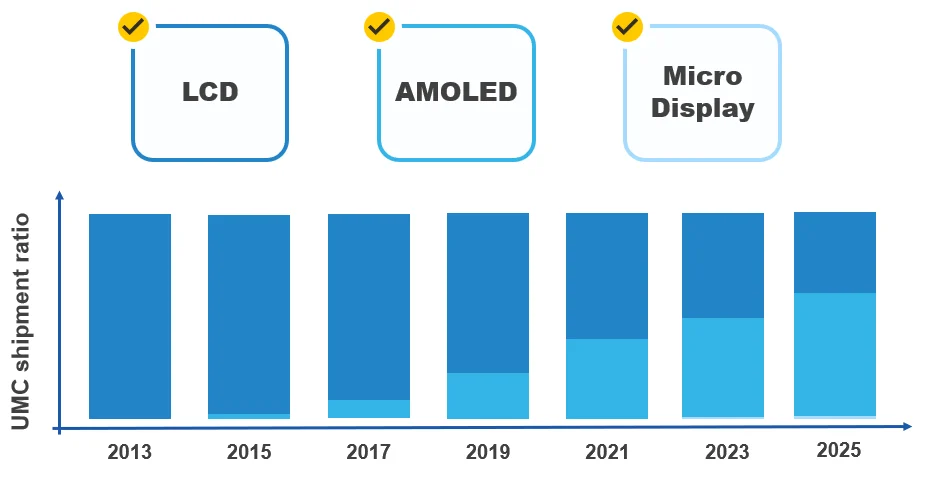
- 2015–2020: The rise of AMOLED in premium smartphones redefined the visual standard. During this phase, DDICs became significantly more complex, requiring sophisticated control over individual pixel voltages rather than just managing global backlight intensity.
- 2021–2025: The industry saw the maturity of 22-nm eHV processes, allowing for more power-efficient DDICs that could handle the high-refresh-rate requirements of modern mobile gaming and high-fidelity video playback.
- 2026 and Beyond: We are currently entering the era of the 14-nm eHV platform. This milestone represents a shift toward advanced FinFET transistors, enabling a 40% reduction in power consumption and a 35% reduction in chip area, critical for the next generation of AR/VR and medical imaging hardware.
Supporting Data: Market Trajectory and Performance Metrics
The economic shift toward AMOLED is undeniable. Market analysis suggests that by 2032, AMOLED technology will command approximately 70% of the global smartphone display market. While the penetration rate in notebook PCs and monitors is currently lower—projected at 30% and 5% respectively—the growth trajectory is clear. As production costs continue to decline and the demand for higher color accuracy increases, AMOLED is poised to become the standard across all personal computing platforms.
The performance gains achieved by moving to smaller nodes are equally compelling. UMC’s latest 14-nm eHV platform, for example, is not merely an incremental update. By leveraging FinFET architecture, it addresses the dual challenge of the "mixed-signal" nature of the DDIC. Because these chips must handle digital data interfaces and memory on one side, and high-voltage analog signals for display driving on the other, the 14-nm process provides the perfect balance of performance and efficiency. This allows for thinner devices with longer battery life, a non-negotiable requirement for the future of wearable tech.

Official Perspective: UMC’s Role in the Ecosystem
While UMC does not manufacture the final display panels themselves, our position as a leading supplier of OLED DDICs places us at the center of the display value chain. We collaborate closely with assembly houses, providing the sophisticated silicon "brains" that power the displays they build.
Our approach is defined by a commitment to process longevity and innovation. We maintain support for mature 8-inch wafer processes, which remain essential for specific cost-sensitive applications, while simultaneously pushing the envelope with our 40-nm to 22-nm and 14-nm eHV processes.
For micro-displays, the industry is currently at a crossroads regarding the "one-chip vs. two-chip" architecture. In a one-chip solution, the DDIC and the pixel array are integrated onto a single silicon substrate. This significantly reduces the interface distance and power loss. UMC is uniquely positioned here; we have the capability to manufacture both the DDIC and the micro-display pixels, offering our clients a streamlined path to high-performance, compact hardware. This dual-capability is what we believe will define the next phase of the AR/VR market.

Implications for the Future of Tech
The implications of these advancements extend far beyond better screens for our phones. We are looking at a future where:
- Immersive AR/VR: High-density, silicon-based displays will finally eliminate the "screen-door effect" in virtual reality, making the experience indistinguishable from reality for the human eye.
- Medical Precision: In fields like robotic surgery or diagnostic imaging, the ability to produce ultra-high-resolution, color-accurate displays on small, portable consoles is a matter of clinical necessity.
- Automotive Evolution: Modern cockpits are becoming massive, wraparound display surfaces. The need for high-reliability, high-voltage-capable DDICs that can operate in extreme temperature environments is driving a new class of automotive-grade silicon.
- Energy Sustainability: As displays consume a large portion of a mobile device’s power budget, the 40% efficiency gains promised by new node transitions directly contribute to the sustainability of the global mobile ecosystem.
The Path Forward
New display types rarely kill off their predecessors entirely; instead, they expand the ecosystem. The continued existence of LCDs, now optimized for specific low-power or cost-effective roles, proves that the "display pie" is growing larger rather than merely swapping flavors.
As we look toward the latter half of the decade, the focus of the semiconductor industry will remain on balancing the conflicting demands of high resolution, low power consumption, and immersive form factors. While AI and data center processing often grab the headlines, the evolution of the interface—the screen you are looking at right now—remains the most vital link in the technological chain. With the continued development of advanced eHV processes and the integration of silicon-substrate display technology, UMC is prepared to power the visual interfaces of tomorrow, ensuring that as display technology evolves, the hardware supporting it remains one step ahead.