In the high-stakes arena of artificial intelligence hardware, the battle for supremacy has shifted from the transistor gate to the package substrate. As the industry grapples with an insatiable demand for AI accelerators, the bottleneck is no longer just lithography—it is the complex art of "stitching" together massive compute dies with high-bandwidth memory (HBM).
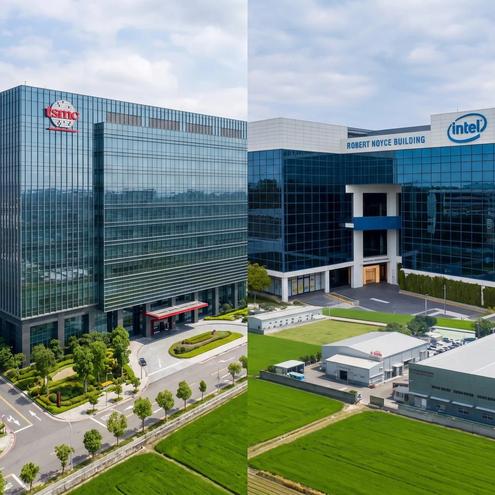
For years, TSMC has held a near-monopolistic grip on the AI ecosystem through its CoWoS (Chip-on-Wafer-on-Substrate) advanced packaging technology. However, cracks in this infrastructure are beginning to show. According to industry analysts, including Neil Shah of Counterpoint Research, TSMC’s reliance on large silicon interposers is creating a significant production bottleneck, providing Intel Foundry with a strategic opening to capture market share from major AI players.
The Main Facts: The Cost of Complexity
The fundamental challenge facing AI chipmakers today lies in the physical constraints of advanced packaging. TSMC’s CoWoS technology, while highly effective, is inherently expensive and risky at scale. By using a large silicon interposer to connect a GPU die to multiple HBM stacks, the process becomes hypersensitive to defects.
"HBM’s reliance on TSMC’s CoWoS silicon interposers carries steep costs with thick packages, yield risk, capacity constraints, and high scrap costs," Neil Shah explained in a recent report.

The economic stakes are staggering. Large silicon dies used in modern AI accelerators already suffer from high defect rates. When an interposer—the foundational layer connecting the compute die to the memory—fails during the final stages of packaging, the entire assembly must be discarded. Because a single GPU is often flanked by eight or more HBM stacks, a defect in the interposer essentially destroys thousands of dollars of premium silicon in one final, catastrophic step.
Chronology of the Packaging Shift
The evolution of this industry struggle can be tracked through a series of strategic technological and geopolitical milestones:
- 2020–2023: TSMC’s CoWoS becomes the gold standard for the AI boom, supporting the meteoric rise of Nvidia, AMD, and Broadcom. Capacity remains tight, and lead times for advanced packaging stretch into months.
- February 2026: Intel and Saimemory announce Z-angle memory (ZAM), a stacked DRAM technology aimed at providing an energy-efficient alternative to traditional HBM.
- Mid-2026: Reports emerge of potential yield issues and capacity constraints within TSMC’s newer CoWoS-L offerings, coinciding with rumors of delays in Nvidia’s next-generation "Vera Rubin" architecture.
- August 2026: Analysts formally identify a shift in strategy among Tier-1 hyperscalers, with Google and MediaTek signaling a move toward Intel’s EMIB (Embedded Multi-die Interconnect Bridge) technology for future TPU (Tensor Processing Unit) iterations.
- Present: The industry enters a phase where "packaging superiority" is viewed by experts like Handel Jones, CEO of International Business Strategies, as being more vital to performance and power efficiency than the migration from 2nm to 1.4nm process nodes.
Supporting Data: Why EMIB Challenges the Status Quo
Intel’s EMIB technology offers a fundamentally different approach to system-in-package (SiP) design. Unlike TSMC’s large-interposer approach, EMIB uses a smaller, localized silicon bridge embedded directly within the organic substrate. This localized connection reduces the surface area susceptible to defects, thereby improving overall package yields.
Counterpoint Research highlights that Intel’s EMIB has been battle-tested in high-volume production, specifically within the company’s Sapphire Rapids and Ponte Vecchio processors. The research firm’s channel checks suggest that Google is positioning itself to be a primary beneficiary of this tech. Specifically, the upcoming TPUv9t (Humufish) and TPUv9t+ (Triggerfish) designs are reportedly slated to utilize Intel Foundry’s EMIB-T, marking a potential "watershed moment" for Intel’s foundry business.

Furthermore, Intel is expanding its footprint in Santa Fe, New Mexico, to support this capacity. This geographic diversification of packaging services is attractive to U.S.-based hyperscalers who are concerned about the concentration of high-end assembly in Taiwan.
Official Responses and Corporate Strategy
The silence from the industry titans speaks volumes. Neither TSMC nor Intel provided formal comment for this report; however, their public actions reveal their respective defensive and offensive postures.
TSMC is not standing still. The foundry is actively iterating on its CoWoS-L architecture, which mirrors some of the efficiency benefits of EMIB by utilizing localized silicon bridges rather than massive interposers. Analyst Mike Demler noted, "I’m inclined to believe TSMC has excellent yields for its CoWoS processes. The newer CoWoS-L may have had some early yield issues, but the company is aggressively optimizing the manufacturing flow."
For Intel, the strategy is about more than just current packaging—it is about the roadmap. By pairing EMIB with future technologies like ZAM and XBM (Cross-batch Memory), which utilizes back-end-of-line thin-film transistors to eliminate interposers entirely, Intel is betting on a "post-interposer" future. Under the leadership of Intel CEO Lip-Bu Tan, the company has telegraphed that memory-integration and heterogeneous computing are the new pillars of their corporate survival.

Implications for the AI Hardware Landscape
The implications of this shift are profound for the broader semiconductor market:
1. The Diversification of Foundries
While Nvidia and AMD remain firmly entrenched in the TSMC ecosystem, the entry of companies like Google (with MediaTek) into the Intel Foundry fold signals a desire for "foundry de-risking." If Intel can prove that its EMIB-T process is not only reliable but cost-effective, it will create a competitive tension that could finally stabilize the runaway costs of AI hardware.
2. The Packaging-First Era
Industry experts agree that we have reached a point of diminishing returns for traditional transistor scaling. As Handel Jones noted, advancements in packaging—integrating multiple chiplets into dense, high-bandwidth configurations—will dictate future performance gains more than shrinking the physical dimensions of the gate. Intel’s focus on Foveros (3D chip-stacking) and EMIB positions it to lead this "packaging-first" design philosophy.
3. Geopolitical Influence
The potential deal between Apple and Intel, as reported by the Wall Street Journal, underscores the political dimension of this shift. With the U.S. government taking a 10% stake in Intel and prioritizing domestic chip security, the foundry business has become a matter of national industrial policy. This institutional backing provides Intel with the runway required to refine its packaging yields, a luxury that smaller competitors lack.

4. The Memory Bottleneck
The integration of HBM remains the single largest point of failure. Intel’s push into ZAM and XBM indicates that they are not content to simply be a foundry for others’ memory; they intend to integrate their own memory-management solutions into the package itself. This could redefine the relationship between processor manufacturers and memory vendors like SK Hynix, Samsung, and Micron.
Conclusion
The narrative that TSMC is invincible is being challenged not by a failure of their lithography, but by the physical limits of their chosen packaging architecture. As AI accelerators continue to grow in complexity, the "interposer problem" identified by analysts will only intensify.
Intel stands at a crossroads. While the company still faces an uphill battle to convince a skeptical market of its execution capabilities, its packaging technologies—specifically EMIB—offer a tangible, high-performance alternative that addresses the primary pain points of the modern AI era. Whether this technical advantage translates into a massive migration of foundry customers remains to be seen, but for the first time in nearly a decade, the path to the top of the AI hardware chain looks significantly more crowded.