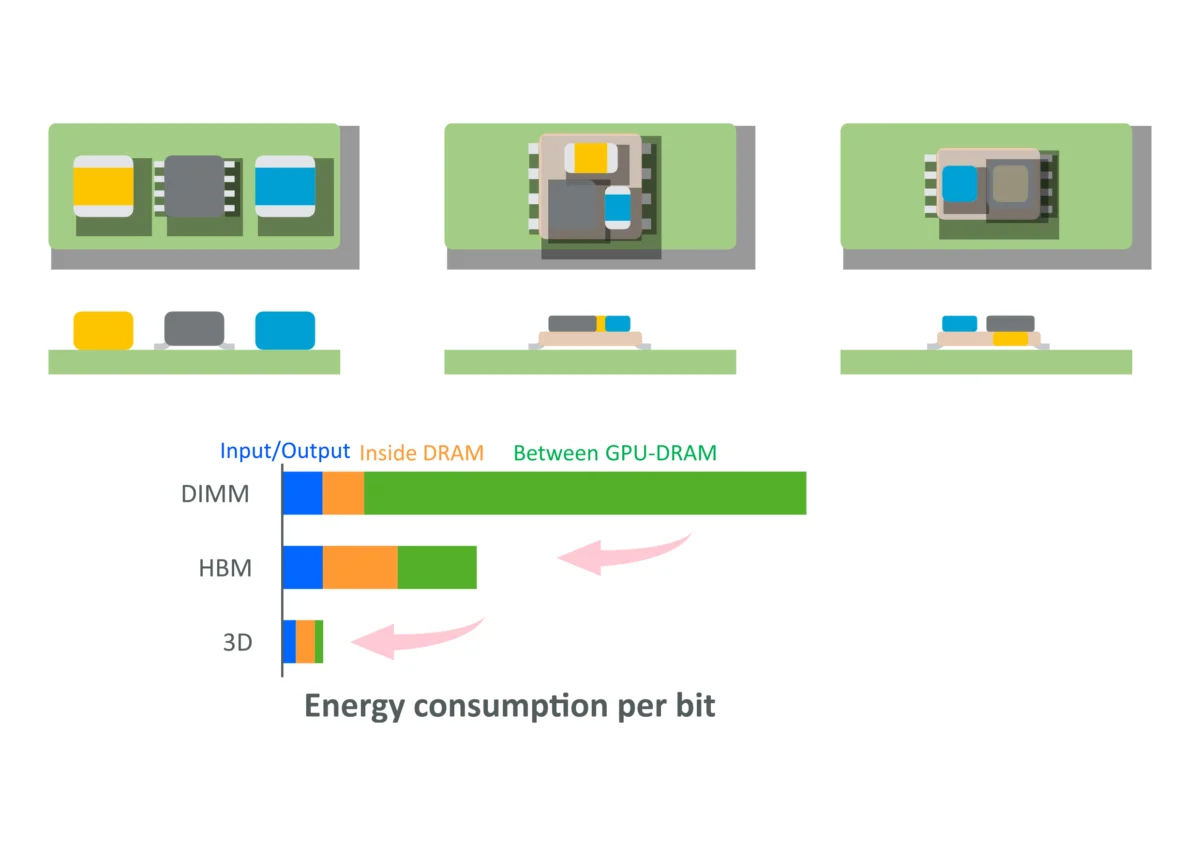
In the high-stakes world of artificial intelligence infrastructure, the most critical electrical path in a server is no longer found on the sprawling surface of a motherboard—it is buried deep within the millimeter-scale architecture of the processor package itself. As AI workloads push compute density to unprecedented levels, the traditional model of board-level power delivery is undergoing a radical, mandatory evolution. Voltage stability, the bedrock of reliable high-performance computing, is now a prisoner of physics, dictated by the proximity of charge to the processor.
Main Facts: The Paradigm Shift in Power Delivery
The fundamental challenge facing modern AI hardware is a collision between shrinking operating voltages and surging current demands. Today’s AI processors typically operate on supply rails approaching 1V, leaving virtually zero margin for error.
In previous generations of silicon, the board-level Power Delivery Network (PDN) was sufficient. Engineers focused on placing voltage regulators and capacitors near the processor to smooth out fluctuations. However, the rise of chiplet architectures and the integration of High-Bandwidth Memory (HBM) have fundamentally altered the landscape. When processors and memory are brought into extreme proximity to maximize data throughput, the electrical path between the power source and the point of load (PoL) becomes a primary design constraint.

The core issue is parasitic inductance. Even a few millimeters of interconnect distance can create enough inductance to cause transient voltage droop—a momentary dip in power that can trigger system instability or data corruption. In the current era of AI, the distance from the nearest decoupling capacitance to the processor is the most critical variable in the entire system.
Chronology: From Board-Level to Package-Integrated Power
The evolution of power delivery follows the trajectory of semiconductor scaling and architectural complexity:
- The Legacy Era (Pre-2015): Power delivery was dominated by the PCB. Large, discrete capacitors were mounted around the processor socket. At these operating speeds, the inductance of the copper traces on the board was manageable.
- The Integration Phase (2015–2020): As HBM and multi-die chiplets emerged, power density increased. Designers began moving decoupling components closer to the processor, but they remained primarily on the surface of the motherboard.
- The Package-Centric Era (2020–2025): With the explosion of generative AI, transient current spikes became too fast for board-mounted solutions to track. The industry began experimenting with embedding passive components into the package substrate.
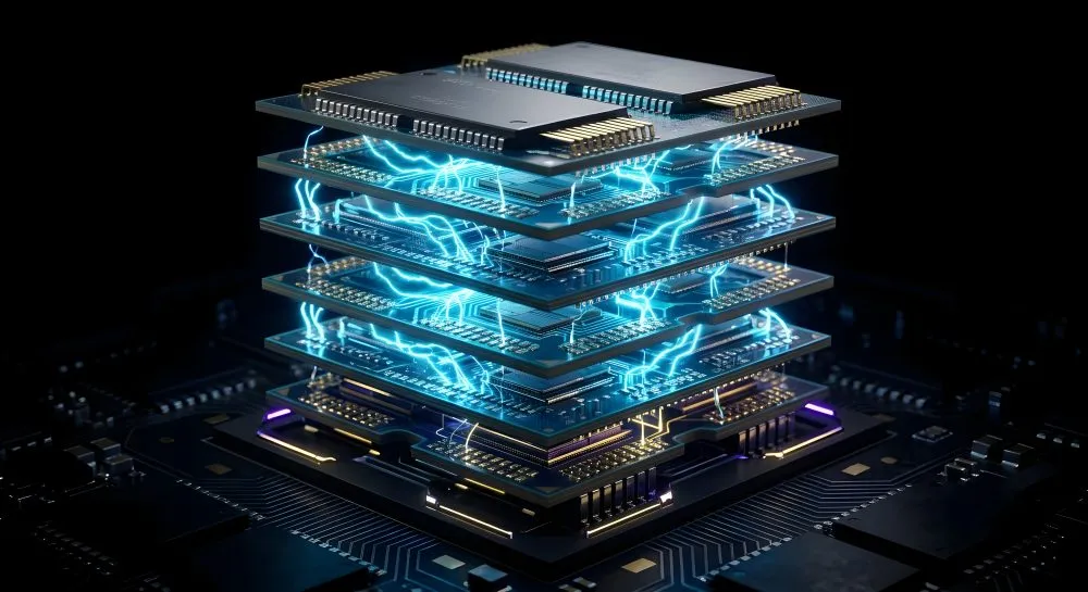
- The Current Frontier (2026–Present): Power delivery is now a unified, hierarchical system. Silicon capacitors are being integrated directly into interposers or substrates, effectively making the package a part of the active electrical circuit.
Supporting Data: Why "More" is No Longer "Better"
A common misconception in power integrity design is that simply adding more capacitors to the board will solve transient issues. Engineering data indicates that this approach reaches a point of diminishing returns quickly.

Once the electrical distance from the capacitor to the die exceeds a certain threshold, the parasitic inductance of the interconnect renders the added capacitance ineffective at high frequencies. For modern AI processors, which generate ultra-fast transient current demands, the "speed of delivery" is dictated by the path length, not the total volume of charge storage.
Recent advancements in silicon capacitor technology allow for capacitance densities of 1.0 µF/mm² or higher. By integrating these components within the package, designers can place stored charge as close as 50–100 µm from the processor. This proximity significantly lowers high-frequency impedance, effectively bridging the gap that longer board-level paths cannot cross. This is not just a marginal improvement; it is a fundamental requirement for the current generation of AI accelerators, which would otherwise experience voltage instability under peak compute loads.
Official Perspectives: The Unified PDN
Industry leaders and architects, including experts from Murata, have emphasized that the board and the package can no longer be treated as separate engineering domains.

"Power integrity now starts inside the package," notes Takaki Murata, Senior VP at Murata. The consensus among hardware architects is that the package has ceased to be a passive carrier; it is now a functional, integral part of the PDN. This shift requires a collaborative design process where silicon architects, power integrity engineers, and package designers work from shared, high-fidelity PDN simulation models.
By treating the processor, the package, and the PCB as a single, holistic electrical system, companies can optimize the current path geometry and decoupling placement to meet the rigorous demands of AI workloads. This unification represents a shift away from silos, requiring teams to harmonize their efforts to avoid the "electrical bottleneck" that could otherwise cripple an AI system’s performance.
Implications for Future AI Infrastructure
The transition to package-integrated power delivery carries significant implications for the future of the semiconductor industry:

1. Cost and Manufacturing Complexity
Integrating passive components directly into the package substrate or interposer adds significant complexity to the manufacturing process. It requires advanced materials and high-precision assembly, which will inevitably impact the Bill of Materials (BOM) for AI-focused server hardware.
2. Design Synergy
The "hierarchy" of power delivery means that design cycles will become more integrated. A change in the processor’s floorplan or memory configuration will immediately trigger a redesign of the package’s power delivery path. We are moving toward a future where the power delivery network is as much a part of the "silicon design" as the compute logic itself.
3. Energy Efficiency
As AI models scale to the trillion-parameter range, energy efficiency is paramount. By minimizing the impedance of the PDN through package-level integration, engineers can reduce the amount of power lost to transient inefficiencies. This "cleaner" power delivery not only improves reliability but also helps in managing the thermal envelopes of massive data centers.

4. The Race for Density
The ability to achieve higher capacitance in smaller footprints is becoming a competitive advantage. Companies that can master the integration of silicon capacitors into advanced packaging will be able to squeeze more performance out of their AI chips, creating a clear technological edge in the race for AI supremacy.
Conclusion: Designing for the Future
The evolution of power delivery is a testament to the sheer scale of the AI revolution. What began as a simple matter of connecting a voltage regulator to a processor has become an intricate, multi-layered discipline of electrical engineering. As we move further into the "Gigawatt Era" of AI, the success of our most powerful systems will depend on our ability to manage the invisible, nanosecond-by-nanosecond fluctuations in power that occur inside the chip.
The package is no longer just a housing; it is the frontline of the power integrity battle. By shrinking the electrical distance between charge and compute, we are clearing the path for the next generation of artificial intelligence, ensuring that when the processor demands power, it receives it instantly—regardless of how fast the workload changes. The future of AI is not just in the silicon, but in the precision with which we deliver the power to make it run.