In the rapidly evolving landscape of artificial intelligence, the physical limitations of hardware are becoming the industry’s most significant hurdle. As AI models grow in complexity and parameter count, the traditional "von Neumann bottleneck"—the speed at which data can move between memory and processing units—is manifesting as a "digital memory wall."
Samsung Electronics, a global titan in semiconductor manufacturing, has officially unveiled a multi-pronged, multi-generational roadmap aimed at dismantling this barrier. By pivoting toward 3D memory architectures, deep-tier process integration, and advanced packaging, Samsung intends to support a future where AI workloads demand a tenfold increase in token throughput by the end of the decade.
The Urgency of the Digital Memory Wall
The demand for memory bandwidth is currently experiencing an exponential surge. According to Leno Park, Vice President of Flash Solutions at Samsung Electronics, the current AI infrastructure is being pushed to its limits. While the industry is currently grappling with the requirements of 2026—supporting roughly 100 tokens per second per user—Samsung is forecasting a much steeper trajectory.
"By the year 2030, we expect to see requirements reach 1,000 tokens per second per user," Park stated during a pre-briefing ahead of the Future of Memory and Storage Summit. This projection underscores a reality that the industry has long suspected: current memory architectures are no longer just a support component; they are the primary bottleneck for generative AI and Large Language Model (LLM) performance. To meet this challenge, Samsung is moving beyond incremental speed bumps, advocating for fundamental structural changes in how memory and processors interact.

Chronology of Innovation: The Roadmap to 2030
Samsung’s strategy is defined by an aggressive development timeline, reflecting the hyper-accelerated nature of the AI hardware market.
Phase 1: The HBM4E Transition (Present – 2026)
Currently, Samsung has entered the sampling phase for HBM4E. This generation of High Bandwidth Memory is being scrutinized by major ecosystem partners, marking a critical transition in the company’s portfolio. Park noted that the development cycle for HBM has "accelerated more than ever," driven by the sheer necessity of keeping pace with hyperscale AI data centers. By 2030, Samsung expects HBM to account for more than 50% of its total DRAM sales, signaling a complete shift in the company’s revenue and R&D focus.
Phase 2: HBM5 and the GAA Breakthrough (2027 – 2028)
Following the current HBM4E rollout, Samsung is targeting a significant leap with HBM5. This generation will move to a 2nm base die utilizing Gate-All-Around (GAA) transistor technology. By shortening interposer channel lengths, Samsung plans to radically improve I/O signaling between the memory base die and the AI accelerator, effectively reducing latency while boosting data transfer rates.
Phase 3: The True 3D Domain (2029 and Beyond)
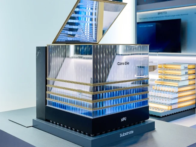
The final stage of the roadmap involves the realization of "zHBM." This marks a departure from the industry-standard 2.5D side-by-side layout. By stacking the AI accelerator directly atop the HBM stack, Samsung intends to create a single, unified 3D domain. This architecture minimizes the physical distance data must travel, which is the foundational solution to the digital memory wall.

Supporting Data and Technical Specifications
Samsung’s technical approach relies on a combination of increased density, improved thermal management, and advanced electrical connectivity.
Advanced Packaging and Connectivity
Samsung’s current HBM design incorporates a 4nm base die, which acts as the foundation for the memory stack. To handle the increased traffic, Samsung has quadrupled the number of internal through-silicon vias (TSVs). Furthermore, the company is employing high-density packaging that utilizes more than 300,000 microbumps. By utilizing smaller joint pitches, Samsung is not only increasing the number of connections but also enhancing the thermal management and reliability of the stack.
The "Chimney" Thermal Mechanism
Thermal management is perhaps the greatest challenge in high-density 3D stacking. To combat the heat generated by these high-performance stacks, Samsung has introduced a "heat pipe block." Described by Park as a "chimney" built over the hot spots of the HBM stack, this mechanism facilitates more efficient heat dissipation. This is a crucial innovation, as heat is the primary enemy of clock speed and component longevity in AI accelerators.
NAND Evolution: The zNAND-O Concept
While HBM receives the lion’s share of attention, Samsung is simultaneously evolving its NAND flash technology. The company introduced zNAND-O, a concept specifically engineered for edge AI. This architecture leverages Samsung’s 10th-generation TLC V-NAND, which features:

- 400+ layer counts: A massive increase in vertical density.
- 11% lateral shrink: Reducing the footprint of individual cells.
- 58% increase in density: Ensuring that edge devices can store massive models locally without relying on cloud round-trips.
Official Perspectives and Industry Implications
The implications of these advancements are profound. By moving to true 3D integration, Samsung claims that its next-generation interface could deliver roughly 8 times the performance of HBM5, 10 times the memory density, and 3 times the energy efficiency, all while cutting thermal resistance by more than half.
However, Samsung is quick to clarify that these milestones cannot be achieved in a vacuum. "Realizing those gains will require close co-design with accelerator partners," Park emphasized. The days of memory manufacturers providing "off-the-shelf" components to CPU/GPU designers are ending. Future architectures require a symbiotic relationship where the memory and the processor are designed as a single, holistic unit.
For the broader tech industry, these developments signal that the "memory wall" is being breached not through better materials alone, but through geometry. By moving from 2.5D layouts to 3D stacking, the latency associated with signal travel is being physically eliminated.
The Broader Context: Why This Matters
The shift toward 3D memory is not merely a technical preference; it is an economic necessity. As AI models transition from simple chatbots to complex autonomous agents, the cost of inference—the process of running a model—is becoming prohibitive. High power consumption and low throughput are the primary contributors to these costs.

By increasing memory bandwidth and energy efficiency, Samsung’s roadmap aims to reduce the "cost per token." This is essential for the democratization of AI. If the hardware can process data more efficiently, the total cost of ownership (TCO) for data centers drops, enabling more companies to deploy sophisticated AI models at scale.
Furthermore, the focus on edge AI via the zNAND-O architecture suggests that Samsung sees a future where the "memory wall" exists not just in the cloud, but on consumer devices. As smartphones and edge servers attempt to run local LLMs, the bottleneck will move to the device’s storage-to-processor interface. By optimizing V-NAND for these specific latency-sensitive tasks, Samsung is positioning itself to be the primary provider of memory for the next generation of AI-integrated hardware.
Conclusion
Samsung’s ambitious roadmap represents a departure from the "speed bump" mentality of the past. By explicitly targeting the digital memory wall and outlining a path that leads to true 3D stacking, the company is signaling that the era of traditional, decoupled memory architectures is coming to a close.
The transition from HBM4E to HBM5 and eventually the zHBM/zNAND-O era will likely define the semiconductor industry’s trajectory for the remainder of the decade. As the world moves toward a future defined by 1,000 tokens per second per user, Samsung’s focus on structural, vertical, and thermal innovation provides a clear, albeit challenging, path forward. Whether the industry can maintain this rapid pace of innovation remains to be seen, but the intent is clear: the wall is not just being climbed; it is being dismantled, layer by layer.