
In the rapidly evolving world of semiconductor engineering, the "power density wall" is no longer a distant theoretical threat—it is the primary bottleneck for the next generation of high-performance computing. As transistors shrink to the atomic scale and 3D-integrated circuits (ICs) become the industry standard, engineers are confronting a dual challenge: macro-scale heat management, which is well-understood, and the increasingly volatile realm of "micro-heat."
Micro-heat refers to the intense, concentrated thermal energy generated at the junction of a semiconductor device. This energy must navigate a complex gauntlet of contacts, packaging, circuit boards, and vias to reach the outside world. Because heat is inherently diffusive and difficult to isolate, measuring how it behaves at the nanometer scale has historically been akin to trying to measure the path of a single drop of water in a turbulent ocean.
Recent breakthroughs from researchers at MIT and Stanford University, however, are beginning to shed light on this elusive phenomenon. By leveraging ultrafast X-rays and quantum-dot sensing, these teams are providing the diagnostic tools necessary to understand—and eventually mitigate—the thermal bottlenecks that threaten to derail the future of Moore’s Law.

The Challenge of Intrusive Measurement
Thermal management at the microscale is notoriously difficult to quantify for two fundamental reasons. First, heat is diffusive; it moves according to thermal conductivity and temperature gradients, often ignoring the neat, linear paths engineers draw in CAD software. Second, traditional instrumentation—such as thermocouples or standard infrared sensors—is inherently intrusive. Introducing a sensor to a sub-micron environment often alters the very heat flow it is intended to measure, creating a "Heisenberg uncertainty" problem for thermal engineers.
To overcome these barriers, a team at MIT has pioneered a sophisticated technique that avoids physical contact by utilizing non-destructive, high-speed probing.
Chronology of a Breakthrough: The MIT Methodology
The MIT research, recently published in Nature Communications under the title "Spatiotemporal mapping of anisotropic thermal transport in GaN thin films via ultrafast X-ray diffraction," represents a significant leap in material characterization.

The Experimental Setup
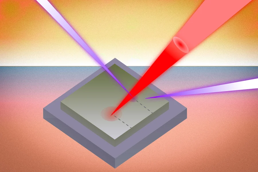
The researchers utilized a "pump-probe" configuration. A high-speed, 343-nm pump laser was used to deliver controlled pulses of heat to a Gallium Nitride (GaN) film—a material of immense interest to the power electronics industry due to its high thermal efficiency.
By syncing this laser with an 11 keV ultrafast X-ray probe, the team was able to observe the material’s atomic response in real-time. As the laser heated the sample, the resulting atomic strain was captured by the X-ray pulses, which possess the unique ability to penetrate multiple material layers. This provided a high-fidelity "movie" of how heat energy dissipated through the lattice, bypassing the limitations of surface-only optical measurements.
Uncovering the "Wrinkle" Effect
The precision of this technique allowed the team to isolate the impact of a single micron-scale defect—a "wrinkle" in the GaN thin film. Their findings were startling:

- Fourfold Reduction: The team measured a fourfold decrease in heat dissipation directly across the wrinkle defect.
- Anisotropic Disruption: They discovered that the defect caused heat to spread unevenly, creating a directional bias in thermal transport that standard design models—which assume uniform material properties—completely fail to account for.
- Performance Deterioration: Even in materials designed for efficiency, these tiny processing defects were found to be responsible for a 25% drop in overall thermal dissipation capacity.
Supporting Data and the Limitations of Current Methods
For decades, engineers have relied on Time-Domain Thermoreflectance (TDTR) to map thermal properties. While TDTR is a gold standard for surface-level characterization, it is insufficient for modern 3D-ICs, which may contain five or more stacked layers. Because TDTR relies on optical reflection, it lacks the "depth perception" needed to observe thermal transport in buried interfaces.
Similarly, infrared (IR) thermography, while useful for macroscopic PCB analysis, lacks the temporal and spatial resolution required to capture the nanosecond-scale fluctuations occurring within an active semiconductor junction.
The MIT technique fills this vacuum, providing the industry with a way to validate thermal models for multilayered, heterogeneous chip designs. By replacing the "guesswork" of uniform thermal modeling with empirical, spatiotemporal mapping, designers can finally account for the microscopic physical disturbances that impede cooling.

Quantum Dots: The Stanford Approach to Entropy
While the MIT team focused on structural mapping, researchers at Stanford University have approached the problem of heat dissipation from the perspective of information theory and entropy.
In their study published in Nature Physics, the Stanford team explored how energy is lost at the most fundamental level using quantum dots—nanocrystals that exhibit unique light-emitting properties. By driving these dots far from equilibrium with a laser field, the team was able to measure "entropy production"—a quantitative metric describing the energy cost of information processing.
"When the field is off, the blinking of a quantum dot follows a certain statistical pattern," explained Yuejun Shen, the study’s lead author. "When the field is on, there’s another pattern. This is how they induced the non-equilibrium state and made the experiment represent information dissipation."

By combining this experimental data with machine learning, the team developed a physics-based model to calculate exactly how much energy is "wasted" as heat during the switching process. This is critical for the next generation of computing, where the energy required to flip a bit is becoming a major component of the overall thermal budget.
Implications for the Semiconductor Industry
The intersection of these two research paths—MIT’s structural thermal mapping and Stanford’s entropy-based dissipation analysis—signals a paradigm shift in how we build high-power electronics.
1. Improved Reliability in 3D-ICs
As we move toward chiplet-based architectures and 3D stacking, the "thermal coupling" between layers becomes the greatest risk to system longevity. The MIT findings suggest that manufacturers must move beyond assuming "average" thermal conductivity. Future manufacturing processes will likely require in-situ metrology to detect the "wrinkles" and defects that the MIT study identified as major thermal inhibitors.

2. Designing for Anisotropy
Traditional thermal management software assumes isotropic heat spread. However, the MIT data proves that in the presence of even minor manufacturing defects, heat flow is highly anisotropic. Designing cooling solutions (like integrated microfluidics or advanced thermal interface materials) will require software that understands these directional biases.
3. The Energy-Information Tradeoff
The Stanford research underscores that energy dissipation is not just a physical problem—it is an information problem. As we push toward exascale computing, the entropy produced by every gate transition represents a hard floor on energy efficiency. By measuring entropy production, engineers can optimize the "cost" of information storage and transfer, leading to more efficient logic architectures.
Conclusion: The Path Forward
The ability to measure heat at the nanoscale is no longer a luxury; it is a necessity. As power management moves from the macro-level of heat sinks and fans to the micro-level of lattice-structure integrity and quantum entropy, the tools developed by the teams at MIT and Stanford will become essential.

While these technologies are currently in the laboratory phase, their translation to industrial metrology could redefine the limits of power density. By shining a light on the invisible, researchers are ensuring that the next generation of semiconductors won’t just be faster—they will be cooler, more reliable, and fundamentally more efficient. The era of "blind" thermal design is ending, replaced by an age of atomic-scale precision.