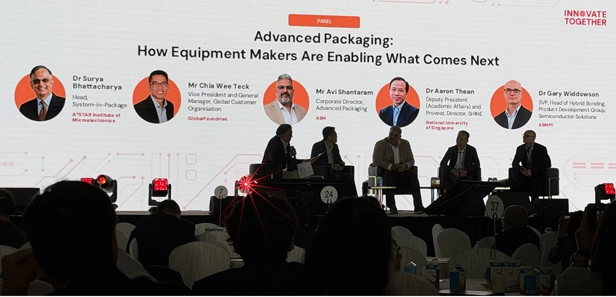
As the semiconductor industry hits the physical limitations of traditional transistor scaling, the mantle of progress has shifted to advanced packaging. At ASTAR’s Innovate Together 2026* summit in Singapore, a coalition of industry titans—including KLA, ASM, ASMPT, and the National University of Singapore (NUS)—converged to address a mounting paradox: the next generation of AI-driven hardware requires packages that are simultaneously growing in physical footprint while demanding interconnect pitches that shrink to the atomic level.
This transition marks a departure from packaging as a mere "afterthought" to its status as the foundational pillar of system design. As Surya Bhattacharya, head of system-in-package at A*STAR’s Institute of Microelectronics (IME), noted, the integration of multiple dies and complex functionalities is now the only viable path to satisfying the insatiable hunger of modern AI computing.
Main Facts: The Great Convergence
The primary challenge facing the semiconductor ecosystem today is the need to harmonize disparate manufacturing disciplines. Advanced packaging is no longer just about assembly; it is an integrated engineering discipline that merges materials science, bonding chemistry, metrology, optical interconnects, and system-level architecture.
The core dilemma is twofold. First, high-performance computing (HPC) demands larger packages, often pushing past the 1x reticle limit to accommodate vast arrays of memory and logic. Second, the drive for lower latency and higher bandwidth necessitates finer interconnect pitches, where even a microscopic particle can compromise an entire system’s reliability. This "large-area, high-density" requirement creates a nightmare for manufacturing yield, as traditional inspection and assembly tools struggle to maintain uniformity across such expansive surfaces.

Chronology of the Packaging Evolution
To understand the current urgency, one must view the evolution of the chip architecture landscape over the last decade:
- 2015–2018: The Era of 2.5D Integration. Industry focus centered on silicon interposers and TSV (Through-Silicon Via) technology to connect HBM to GPUs, marking the initial move away from monolithic chip design.
- 2019–2022: The Emergence of Chiplets. The industry transitioned toward modular chiplet architectures, allowing for heterogeneous integration. However, thermal management and basic interconnect density remained the primary constraints.
- 2023–2025: The Rise of Hybrid Bonding. As density needs surged, the industry began pivoting from standard micro-bumps to copper-to-copper hybrid bonding, enabling vertical 3D stacking with drastically reduced pitch sizes.
- 2026 and Beyond: The Panel-Level/Optical Era. We are currently witnessing the migration toward panel-level packaging to support massive, multi-reticle designs, while simultaneously integrating photonics directly into the package stack to solve the "data bottleneck" of electrical wiring.
Supporting Data and Technical Hurdles
The transition to hybrid bonding is the most significant technological pivot in recent memory. Unlike conventional thermal compression bonding (TCB), which utilizes solder, hybrid bonding facilitates direct copper-to-copper contact.
The Physics of the Interface
The data suggests that the "process window" for successful hybrid bonding is exceptionally narrow. Key variables include:
- Surface Roughness: Even nanometer-scale irregularities can prevent electrical contact.
- CMP Dishing: Chemical mechanical polishing must be precise to within a few angstroms to ensure that the copper interconnects are perfectly flush with the surrounding dielectric material.
- Contamination Control: A particle that would be negligible in a standard package can create a massive void at the bonding interface, leading to "open" circuits or catastrophic failure under thermal stress.
As Gary Widdowson, CTO of ASMPT, emphasized, hybrid bonding is not a "silver bullet" that will immediately render TCB obsolete. Instead, both technologies will coexist. TCB remains the cost-effective workhorse for many applications, while hybrid bonding is reserved for the high-density frontiers where electrical performance requirements outweigh the current, higher manufacturing costs.

The Rise of Panel-Level Packaging (PLP)
With package sizes potentially reaching 9x the reticle area, the 300-mm wafer is becoming a bottleneck. The industry is currently evaluating a migration to panel-based formats, with 510 x 515 mm emerging as a potential standard. However, this transition is fraught with manufacturing risks. Large, thin panels are prone to warpage, and the sheer area increases the statistical probability of a fatal defect occurring somewhere on the substrate.
Official Responses and Strategic Perspectives
Industry leaders at the Singapore summit were unanimous in their assessment: the "siloed" approach to manufacturing is dead.
KLA’s Perspective:
Chia Wee Teck, VP and GM at KLA, argued that inspection cannot be a "gatekeeper" at the end of the line. "If you can’t see it, you can’t measure it, you can’t control it," Chia stated. KLA’s strategy involves building an automated, continuous feedback loop where metrology data is fed back into the lithography and etching processes in real-time. By monitoring copper surface profiles and bond voids early, manufacturers can adjust process parameters on the fly, preventing "yield drift."
ASM’s Perspective:
Avi Shantaram emphasized that the industry must view hybrid bonding as a holistic interface engineering problem. It is not just about the bonding equipment; it is about the entire upstream flow—precursor chemistry, atomic layer deposition (ALD), and surface treatment must be perfectly synchronized.

NUS’s Perspective:
Aaron Thean of NUS highlighted the looming bottleneck of data movement. With data rates pushing toward 400 Gb/s per lane, copper-based electrical interconnects are running out of steam. The integration of photonics—PICs (Photonic Integrated Circuits) and EICs (Electronic Integrated Circuits)—into the package is now a top-tier priority. This requires an entirely new set of packaging challenges, including the precise alignment of fiber arrays, microlenses, and lasers within a hermetically sealed, thermally stable environment.
Implications for the Semiconductor Ecosystem
The implications of these advancements are profound, touching on everything from economics to global supply chain resilience.
- The End of the "One-Size-Fits-All" Package: We are entering an era of extreme specialization. The "packaging stack" will become the primary differentiator for companies like NVIDIA, AMD, and Intel, potentially more so than the underlying transistor process itself.
- Economic Realignment: The transition to larger panel-level formats requires massive capital expenditure (CapEx) in new fabrication facilities. This will likely concentrate the advanced packaging market among the largest players (TSMC, Intel, Samsung, and ASE), as the cost of entry rises exponentially.
- Standardization Requirements: The industry must reach a consensus on panel sizes and interface standards. Without a common framework, the ecosystem risks fragmentation, where proprietary packaging standards prevent the interoperability of chiplets from different vendors.
- A Shift in Reliability Models: With 3D-stacked AI systems, reliability is no longer just about the chip; it is about the "system-in-package." The industry must develop new, accelerated testing methodologies that account for the unique thermal-mechanical stresses of vertical stacking and co-packaged optics.
Conclusion
The path forward for AI is paved with the complexities of advanced packaging. By shifting from traditional, iterative improvements to a unified, data-driven approach that integrates materials science with massive-scale manufacturing, the industry aims to keep pace with the exponential growth of AI models. As the experts at Innovate Together 2026 concluded, the success of the next decade of computing will be measured not just in how many transistors we can shrink, but in how seamlessly we can connect, package, and protect the complex systems of the future.